Hardware Design
Module Pin Diagram
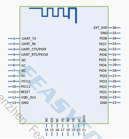
Pin Description
Pin |
Pin Name |
Type |
Pin Descriptions |
|---|---|---|---|
1 |
UART_TX |
O |
UART Data Pin (Transmit) |
2 |
UART_RX |
I |
UART Data Pin (Receive) |
3 |
UART_CTS |
I |
UART Flow Control Pin (Clear To Send) |
4 |
UART_RTS |
O |
UART Flow Control Pin (Request To Send) |
11 |
RESET |
I |
Reset Pin (Active-Low) |
12 |
VDD |
Power |
Power Supply, 3.3V |
13 |
GND |
GND |
GND |
15 |
ICE |
I/O |
Programming Pin (In-Circuit Emulator) |
29 |
I2C_CLK |
I/O |
I²C Clock |
30 |
I2C_DTA |
I/O |
I²C Data |
32 |
Work |
O |
Outputs square wave when BT not connected; Outputs high level when BT connected. |
33 |
STATUS |
O |
Outputs low level when BT not connected; Outputs high level when BT connected. |
36 |
EXT_ANT |
ANT |
Change the 0Ω resistor near the antenna to connect an external Bluetooth antenna. |
Hardware Design Notes
In simple test environment, the module can be used for basic testing and operation by simply connecting VDD, GND, UART_RX, and UART_TX.
If the MCU needs to obtain the Bluetooth module’s connection status, connect to the STATUS pin.
Please submit the schematic diagram to Feasycom for review upon completion to ensure optimal Bluetooth range performance.