Hardware Design
Module Pin Diagram
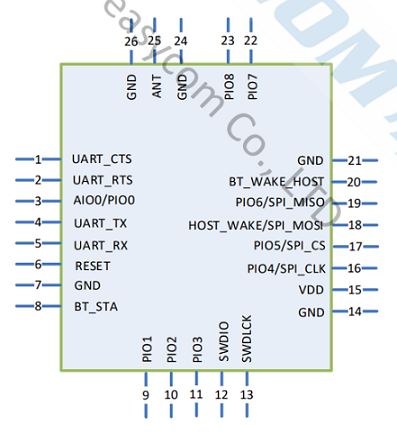
Pin Description
Pin |
Pin Name |
Type |
Pin Descriptions |
|---|---|---|---|
1 |
UART_CTS |
I/O |
Serial Port Flow Control Pin |
2 |
UART_RTS |
I/O |
Serial Port Flow Control Pin |
3 |
AOI0/PIO0 |
I/O |
ADC |
4 |
UART_TX |
O |
Serial Port Data Pin |
5 |
UART_RX |
I |
Serial Port Data Pin |
6 |
RESET |
I |
Low-Level Reset |
7 |
GND |
GND |
GND |
8 |
STATUS |
O |
Low level : Bluetooth is disconnected. |
12 |
SWDIO |
I/O |
Programming Pin |
13 |
SWDCLK |
I |
Programming Pin |
15 |
VDD |
Power |
Power supply: 3.3V. |
16 |
SPI_CLK |
I/O |
SPI_CLK PIN |
17 |
SPI_CS |
I/O |
SPI_CS PIN |
18 |
HOST_WAKE |
O |
HOST Controlled Pin: |
19 |
SPI_MISO |
O |
SPI_MISO PIN |
20 |
BT_WAKE_HOST |
O |
High level wakes up the BT. |
25 |
ANT |
ANT |
Changing the 0-ohm resistor near the antenna allows |
Hardware Design Note
The module can be used by connecting VDD/GND/BT_STA/UART_RX/UART_TX.
If the MCU needs to obtain the connection status of the Bluetooth module, it is necessary to connect the BT_STA pin.
If there is a low-power consumption requirement, please connect the BT_WAKE_HOST and HOST_WAKE_BT pins.
After completing the schematic diagram, please send it to Feasycom for review to avoid the Bluetooth range failing to reach the optimal performance.