Hardware Design
Module Pin Diagram
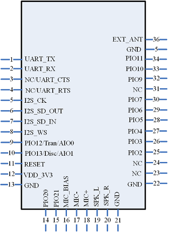
Module Pin Description
Pin |
Pin Name |
Type |
Pin Descriptions |
|---|---|---|---|
1 |
UART_TX |
O |
UART TX |
2 |
UART_RX |
I |
UART RX |
5 |
I2S_CLK |
I/O |
I2S bit clock |
6 |
I2S_OUT |
O |
I2S data output |
7 |
I2S-IN |
I |
I2S data input |
8 |
I2S-WS |
I/O |
Frame Sync Clock |
11 |
RESET |
I |
active-low reset |
12 |
VDD_3V3 |
I |
3.3V power supply |
13 |
GND |
GND |
|
16 |
MIC_BIAS |
O |
microphone bias voltage |
17 |
MIC- |
I |
MIC negative |
18 |
MIC+ |
I |
MIC positive |
19 |
SPK_L |
O |
left channel |
20 |
SPK_R |
O |
right channel |
32 |
PIO_9 |
I/O |
operating status indicator Pin |
33 |
PIO_10 |
I/O |
connection indicator Pin |
36 |
ANT |
external antenna Pin |
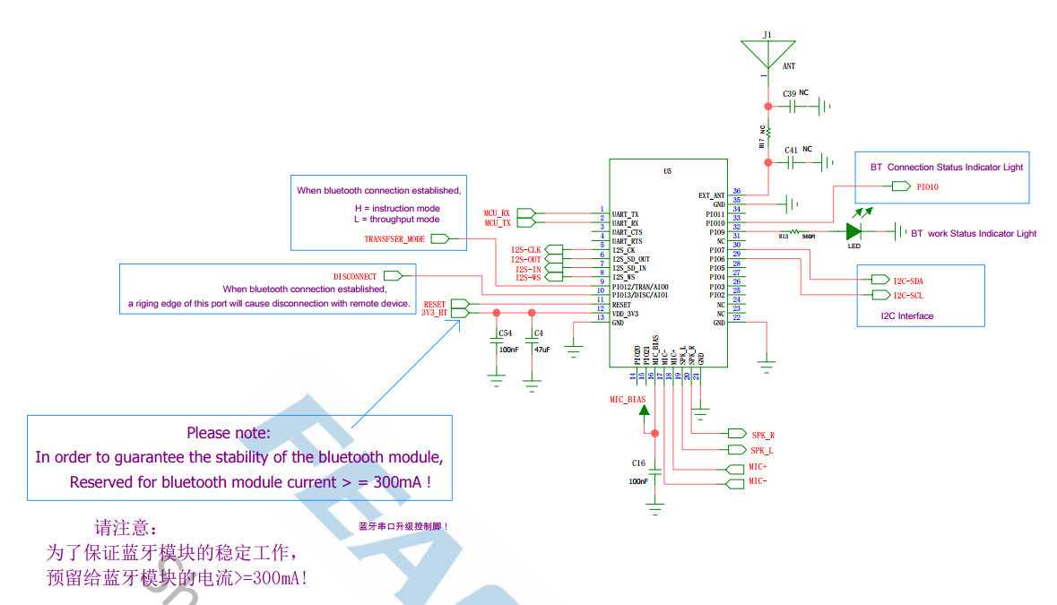
Application Schematic
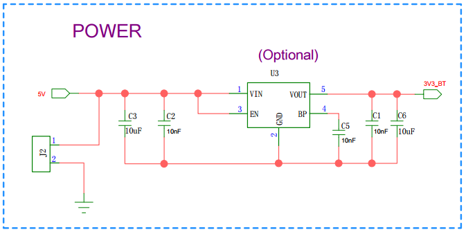
Power-on Circuit Design
To ensure the stable operation of the Bluetooth module, the power supply for the VDD_3V3 pin must reserve a current of ≥ 300mA for the Bluetooth module.
If the power supply is converted from 5V to 3.3V, you can refer to the following optional recommended schematic diagram for design:
Hardware Design Note
For the module’s simple test environment, you only need to connect VDD / GND / UART_RX / UART_TX to test and use it.
After completing the PCB circuit schematic, please contact the staff of Feasycom for review to prevent the Bluetooth range from failing to reach the optimal performance.