Hardware Design
Module Pin Description
FSC-BT9101AI
Module Pin Diagram:
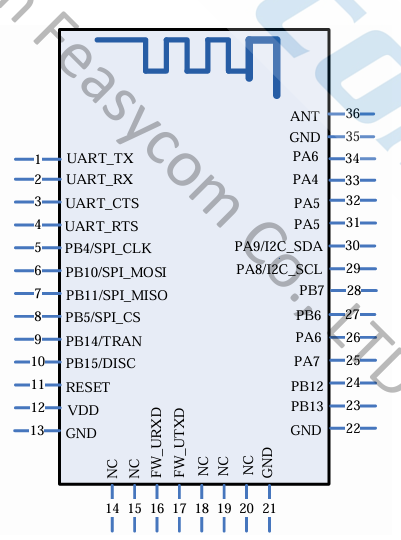
Pin Description:
Pin |
Pin Name |
Type |
Descriptions |
|---|---|---|---|
1 |
UART_TX |
I/O |
UART Data Out. |
2 |
UART_RX |
I/O |
UART Data In. |
3 |
UART_CTS |
I/O |
UART Clear to Send (active low). |
4 |
UART_RTS |
I/O |
UART Request to Send (active low). |
9 |
Tran/CMD |
I/O |
Host MCU change UART transmission mode.(Default) |
10 |
Disc |
I/O |
Host MCU disconnect Bluetooth.(Default) |
11 |
RESET |
I |
External reset input: Active LOW. |
12 |
VDD |
Power |
Power supply voltage 3.3V~3.6V. |
13 |
GND |
Vss |
Power Ground |
16 |
FW_URXD |
I/O |
Firmware download RXD. |
17 |
FW_UTXD |
I/O |
Firmware download TXD. |
29 |
I2C_SCL |
I/O |
I2C_SCL |
30 |
I2C_SDA |
I/O |
I2C_SDA |
31/32 |
PA5 |
I/O |
LED |
33 |
PA4 |
I/O |
BT Status |
36 |
EXT_ANT |
O |
RF signal output. |
FSC-BT9104DI
Module Pin Diagram:
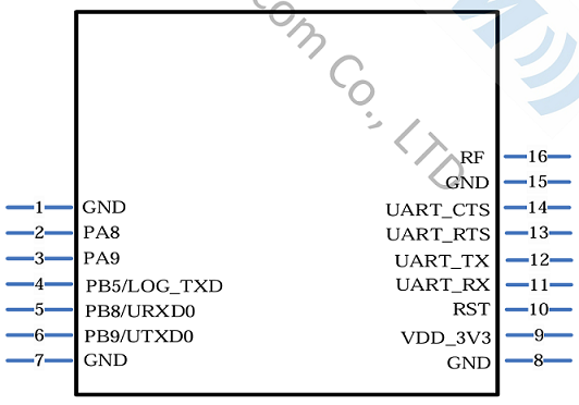
Pin Description:
Pin |
Pin Name |
Type |
Pin Descriptions |
|---|---|---|---|
1 |
GND |
GND |
Power Ground |
3 |
PA9 |
I/O |
BT Status, |
5 |
FW_URXD |
I |
Firmware download RXD. |
6 |
FW_UTXD |
O |
Firmware download TXD. |
8 |
GND |
Vss |
Power Ground |
9 |
VDD_3V3 |
VDD |
Power supply voltage 3.3V |
10 |
RST |
I |
External reset input: Active LOW. |
11 |
UART_RX |
I |
UART data input. |
12 |
UART_TX |
O |
UART data output. |
13 |
UART_RTS |
I/O |
UART request to send active low. |
14 |
UART_CTS |
I/O |
UART clear to send active low. |
15 |
GND |
Vss |
Power Ground |
16 |
RF |
RF_IN/OUT |
Bluetooth 50ohm transmitter output/receiver input. |
Hardware Design Note
In simple test environment, the module can be used for basic testing and operation by simply connecting VDD, GND, UART_RX, and UART_TX.
If the MCU needs to obtain the connection status of the Bluetooth module, it needs to be connected to the STATUS pin.
After drawing the schematic diagram, please send it to Feasycom for review to avoid Bluetooth distance not achieving the best effect.