Hardware Design
Module Pin Diagram
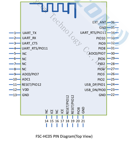
Pin Description
Pin |
Pin Name |
Type |
Pin Descriptions |
|---|---|---|---|
1 |
UART_TX |
O |
Serial Transmitter Data |
2 |
UART_RX |
I |
Serial Receiver Data |
3 |
UART_CTS |
I/O |
UART Clear to Send(no connection request) |
4 |
UART_RTS |
I/O |
UART Request to Send(no connection request) |
9 |
Disc/USB_DM/PIO0 |
I/O |
Disconnect the connecting pin |
11 |
RESET |
I |
Active-low reset input |
12 |
VDD |
Power |
Power supply voltage 3.3V, LDO power supply preferred |
13 |
GND |
GND |
GND |
15 |
ICE |
I/O |
Writing firmware pin |
32 |
LED |
O |
Bluetooth not connected to output square wave, Bluetooth connected to output high level |
33 |
STATUS |
O |
Connection state, output. H=Connected , L=No connection |
34 |
Tran/USB_DP/PIO1 |
O |
UART Mode Control Pin: H = Command Mode; L = Transparent Transmission Mode |
36 |
EXT_ANT |
ANT |
Changing the 0 ohm resistance near the antenna, it is possible to connect a Bluetooth antenna externally |
Hardware Design Notes
In simple test environment, the module can be used for basic testing and operation by simply connecting VDD, GND, UART_RX, and UART_TX.
If the MCU needs to obtain the connection status of the Bluetooth module, it needs to be connected to the STATUS pin.
After drawing the schematic diagram, please send it to Feasycom for review to avoid Bluetooth distance not achieving the best effect.