Hardware Design
Module Pin Diagram
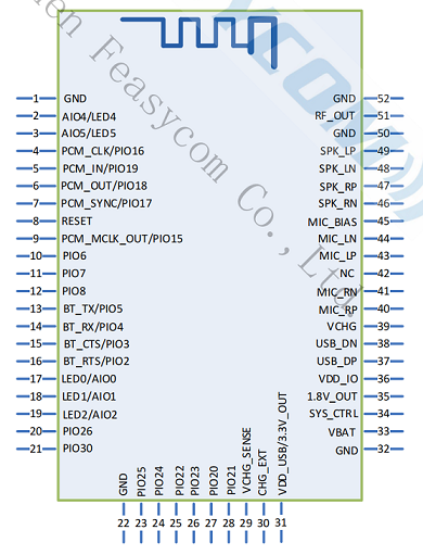
Pin Description
BT1038x |
Pin Name |
Type |
Pin Descriptions |
|---|---|---|---|
4 |
I2S_CLK |
I/O |
I2S BCLK |
5 |
I2S_IN |
I |
I2S DATA IN |
6 |
I2S_OUT |
O |
I2S DATA OUT |
7 |
I2S_WS |
I/O |
I2S SYNC |
8 |
RESET |
I |
Low level reset |
13 |
UART_TX |
O |
UART_TX |
14 |
UART_RX |
I |
UART_RX |
15 |
UART_CTS |
I/O |
UART flow control pin (not required by default) |
16 |
UART_RTS |
I/O |
default as power amplifier control pin |
17 |
LED0 |
I/O |
General-purpose analog/digital input or output. |
18 |
LED1 |
I/O |
General-purpose analog/digital input or output |
32 |
GND |
GND |
GND |
33 |
VDD |
VDD |
3.3V power supply, it is recommended to use LDO |
34 |
VREG_IN |
I |
Power on/off pin |
36 |
VDD_IO |
I |
pio supply |
43 |
MIC_LP |
Audio |
MIC0/Line_IN differential L input, positive |
44 |
MIC_LN |
Audio |
MIC0/Line_IN differential L input, negative |
45 |
MIC_BIAS |
Audio |
MIC Power Supplies |
46 |
SPK_RN |
Audio |
Headphone/speaker differential R output, negative |
47 |
SPK_RP |
Audio |
Headphone/speaker differential R output, positive |
48 |
SPK_LN |
Audio |
Headphone/speaker differential L output, negative |
49 |
SPK_LP |
Audio |
Headphone/speaker differential L output, positive |
51 |
EXT_ANT |
ANT |
External antenna connect pin |
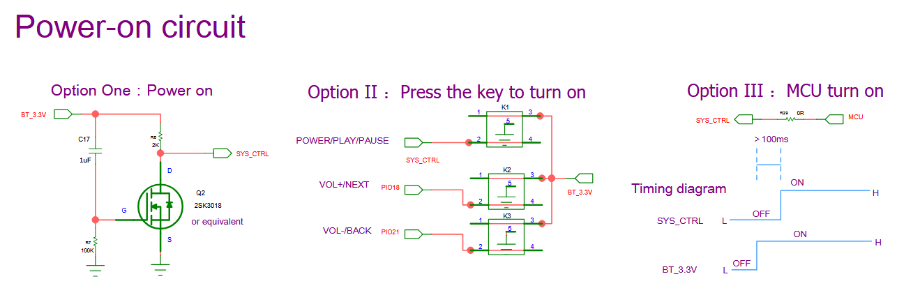
Power-on Circuit Design
The FSC-BT1038X module has three options for power on, which are: delayed power on circuit, button on/off circuit, and MCU controlled power on/off circuit. As shown in the following figure:
Hardware Design Note
simple testing environment, just connect VDD / VDD_IO / SYS_CTRL / GND / UART_RX / UART_TX.
After drawing the PCB circuit schematic, please send it to Feasycom for review to avoid suboptimal Bluetooth distance.