Hardware Design
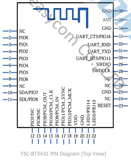
Module Pin Diagram
Pin Description
Pin |
Pin Name |
Type |
Pin Descriptions |
|---|---|---|---|
31 |
UART_TX |
O |
UART data pin |
32 |
UART_RX |
I |
UART data pin |
23 |
RESET |
I |
Active-low reset |
19 |
VDD |
Power |
3.3V power supply. |
20 |
GND |
GND |
GND |
28 |
SWCLK |
I/O |
Programming pin |
29 |
SWDIO |
I/O |
Programming pin |
8 |
SLP_IND |
O |
After Bluetooth connection, the module pulls low to notify the customer’s MCU to exit sleep mode, and outputs serial data with a 10ms delay. |
7 |
WAKE_UP |
I |
When the MCU pulls high, the module enters sleep mode. |
21 |
LED |
O |
Outputs a square wave when Bluetooth is disconnected. |
22 |
STATUS |
O |
Low level : Bluetooth is disconnected. |
Hardware Design Note
The module can be used by simply connecting VDD/GND/STATUS/UART_RX/UART_TX.
If the MCU needs to obtain the connection status of the Bluetooth module, the STATUS pin (Pin 22) must be connected.
If the user needs to check the working status of the module, the LED pin (Pin 21) must be connected.
If low-power consumption is required, connect Pin 8 (SLP_IND) and Pin 7 (WAKE_UP); leave these pins floating if low-power consumption is not needed.
After completing the schematic diagram, please send it to Feasycom for review to ensure the Bluetooth communication distance reaches the optimal performance.