Hardware Design
Module Pin Diagram
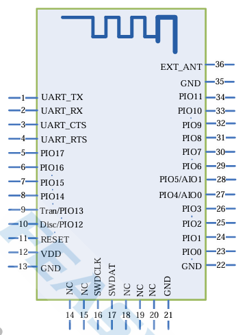
Pin Description
Pin |
Pin Name |
Type |
Pin Descriptions |
|---|---|---|---|
1 |
UART_TX |
O |
UART data pin |
2 |
UART_RX |
I |
UART data pin |
3 |
UART_RTS |
I/O |
Serial Port Flow Control Pin |
4 |
UART_CTS |
I/O |
Serial Port Flow Control Pin |
9 |
RESTORE |
I |
Reset configuration |
11 |
RESET |
I |
Active-low reset |
12 |
VDD |
Power |
3.3V power supply.LDO (Low Dropout Regulator) power supply is recommended |
13 |
GND |
GND |
GND |
16 |
SWCLK |
I/O |
Programming pin |
17 |
SWDIO |
I/O |
Programming pin |
32 |
LED |
O |
Outputs a square wave when Bluetooth is disconnected.outputs high level when Bluetooth is connected |
31 |
WAKE_MCU |
O |
Bluetooth in low-power mode wakes up the MCU |
33 |
STATUS |
O |
Outputs low level when Bluetooth is disconnected, and high level when Bluetooth is connected |
34 |
WAKE_BT |
I |
MCU in low-power mode wakes up Bluetooth |
36 |
EXT_ANT |
ANT |
An external Bluetooth antenna can be connected by changing the 0-ohm resistor near the antenna |
Hardware Design Note
The module can be used by simply connectingVDD/GND/STATUS/UART_RX/UART_TX
If the MCU needs to obtain the connection status of the Bluetooth module, the STATUS pin (Pin 10) must be connected.
The module supports GPIO-based wake-up. If the application has low-power consumption requirements, the WAKE_MCU/WAKE_BT pins must be connected.
VDD/GND/RESET/SWCLK/SWDIO serve as the programming interface, and test points may be reserved for debugging and testing purposes.
After completing the schematic diagram, please send it to Feasycom for review to ensure the Bluetooth communication distance reaches the optimal performance.