Hardware Design
Module Pin Diagram
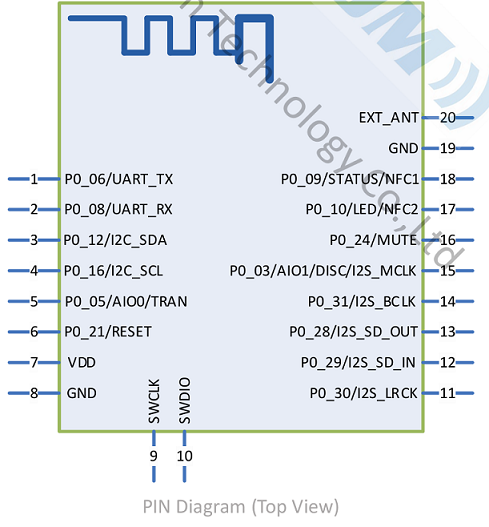
Pin Description
Pin |
Pin Name |
Type |
Pin Descriptions |
|---|---|---|---|
1 |
UART_TX |
O |
UART Data Pin |
2 |
UART_RX |
I |
UART Data Pin |
6 |
RESET |
I |
Active-Low Reset |
7 |
VDD |
Power |
3.3V Power Supply.<LDO power supply is recommended |
8 |
GND |
GND |
GND |
9 |
SWCLK |
I/O |
Programming Pin |
10 |
SWDIO |
I/O |
Programming Pin |
7 |
WAKE_UP |
I |
When MCU pulls high, the module enters sleep mode. |
17 |
LED |
O |
Outputs square wave when Bluetooth is disconnected. |
18 |
STATUS |
O |
Outputs low level when Bluetooth is disconnected. |
20 |
EXT_ANT |
ANT |
Changing the 0Ω resistor near the antenna allows external Bluetooth antenna connection |
Hardware Design Note
The module can be used by simply connecting VDD / GND / STATUS / UART_RX / UART_TX.
If the MCU needs to obtain the connection status of the Bluetooth module, the STATUS pin needs to be connected
After completing the schematic diagram, please send it to Feiyitong for review to avoid the Bluetooth distance not reaching the optimal effect
The module supports wake-up via UART
VDD/GND/RESET/SWCLK/SWDIO are programming ports, and test points can be reserved