Hardware Design
Module Pin Diagram
Pin diagram with FSC-BW246:
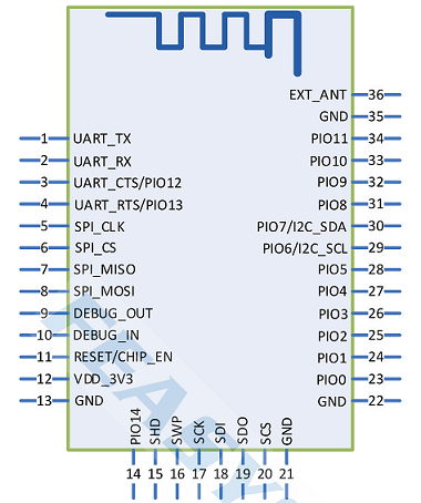
Pin Description
Pin |
Pin Name |
Type |
Descriptions |
|---|---|---|---|
1 |
UART_TX |
O |
UART Data output |
2 |
UART_RX |
I |
UART Data input |
3 |
UART_CTS |
I |
UART clear to send (active low) |
4 |
UART_RTS |
O |
UART request to send (active low) |
9 |
DEBUG_OUT |
I/O |
Debug Interface (Data OUT) |
10 |
DEBUG_IN |
I/O |
Debug Interface (Data IN) |
11 |
RESET/CHIP_EN |
I |
External reset input, active low. |
12 |
VDD_3V3 |
VDD |
Power supply voltage 2.3~3.3V |
13 |
GND |
VSS |
Power Ground |
21 |
GND |
VSS |
Power Ground |
22 |
GND |
VSS |
Power Ground |
32 |
LED0 |
I/O |
Bluetooth is connected to output high |
33 |
LED1 |
I/O |
Wi-Fi is connected to output high level |
35 |
GND |
VSS |
RF Ground |
36 |
EXT_ANT |
O |
RF signal output |
Note: This section provides brief I/O pin descriptions. For detailed descriptions and precautions, please refer to FSC-BW246 Datasheet .
Hardware Interface
GPIO
PWM
UART
SPI SLAVE
I2S Master/Slave
Analog Input/Output
Hardware Design Note
The simple test of the module only requires connecting VDD/GND/UART_RX/UART_TX to be used
After drawing the schematic diagram, please send it to Feasycom for review to avoid the Bluetooth or Wi-Fi distance not achieving the best effect