Hardware Design
Module PIN Diagram
Pin diagram with FSC-BW256B:
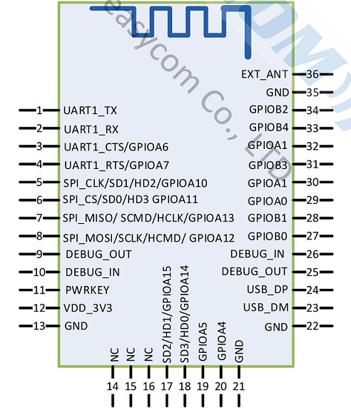
Pin Description
Pin |
Pin Name |
Type |
Descriptions |
|---|---|---|---|
1 |
UART1_TX |
O |
UART data output |
2 |
UART1_RX |
I |
UART data input |
3 |
UART_CTS |
I/O |
UART clear to send (active low) |
4 |
UART_RTS |
I/O |
UART request to send (active low) |
5 |
SPI_CLK/SD1 |
I/O |
SPI_CLK. |
6 |
SPI_CS/SD0 |
I/O |
SPI_CS. |
7 |
SPI_MISO/SCMD |
I/O |
SPI_MISO. |
8 |
SPI_MOSI/SCLK |
I/O |
SPI_MOSI. |
9 |
DEBUG_OUT |
I/O |
Debug Interface (Data OUT) |
10 |
DEBUG_IN |
I/O |
Debug Interface (Data IN) |
11 |
PWRKEY |
I |
Module power-on pin; |
12 |
VDD_3V3 |
VDD |
3.3V power supply |
13 |
GND |
VSS |
Power Ground |
17 |
SD2 |
I/O |
SDIO D2 as master; SDIO D1 as slave. |
18 |
SD3 |
I/O |
SDIO D3 as master; SDIO D0 as slave. |
21 |
GND |
VSS |
Power Ground |
22 |
GND |
VSS |
Power Ground |
23 |
USB_DM |
I/O |
USB data D- |
24 |
USB_DP |
I/O |
USB data D+ |
32 |
LED0 |
I/O |
Bluetooth is connected to output high |
33 |
LED1 |
I/O |
Wi-Fi is connected to output high level |
35 |
GND |
VSS |
RF Ground |
36 |
EXT_ANT |
ANT |
Wi-Fi 2.4G radio frequency |
Note: This section provides brief I/O pin descriptions. For detailed descriptions and precautions, please refer to FSC-BW256B Datasheet .
Hardware Interface
GPIO
PWM
UART
USB 2.0
SPI
SDIO 3.0
Hardware Design Note
The simple test of the module only requires connecting VDD/GND/UART_RX/UART_TX to be used.
After drawing the schematic diagram, please send it to Feasycom for review to avoid the Bluetooth or Wi-Fi distance not achieving the best effect.